![Multiplexer Report [PDF]](https://pdfs.asia/img/200x200/multiplexer-report.jpg)
16 0 143 KB
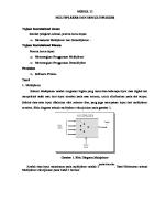
TITLE : MULTIPLEXER INSTRUCTION AIMS: The trainees must be able to 1. Design function of Multiplexer 2. Donstruct the internal circuitry of Multiplexer TOOLS, EQUIPMENTS AND MATERIALS: 1. 2. 3. 4. 5.
Breadboard Power supply IC 7408, 7432, 7404, 7411(3 input AND gate), 74151 LED Jumper wires
DRAWING, DATA, TABLE Refer to pages with the procedure instruction GENERAL INSTRUCTION: A multiplexer is a device capable of funneling data lines into a single line transmission to another point. The multiplexer has two or more digital inputs signals connected to its input. Control signals are also input to hell which data-inputs line to select for transmission. D0 D1 D2 D3
Experiment 1 : 2 Line Multiplexer Procedure: 1. IC 7404, 7432, 7408 must be installed in the logic lab breadboard 2. the circuit was constructed as figure 1 3. Data must be set as switch like in multiplexer truth table. Output at LED must recorded in table 1
A 0 1 X X
INPUTS B X X 0 1
C 0 0 1 1 TABLE 1.
OUTPUTS 0 0 0 0
1(B) 1(B) 1(A) 1(A)
Experiment 2 : 4 Line Multipplexer. Procedure: 1. Ic 7411,7408,7404 was installed in the logic breadboard. 2. The circuit was construct in figure above . 3. Data must be set up as switch like input truth table ouput also must be record in table 2
.
INPUTS D0
D1
D2
D3
S0
S1
0 1 0 1 0 1 0 1 0 1 1 1 1 1 1 1
0 0 1 1 0 0 1 1 0 0 0 0 1 1 1 1
0 0 0 0 1 1 1 1 0 0 1 1 0 0 1 1
0 0 0 0 0 0 0 0 1 1 0 1 0 1 0 1
0 1 0 1 0 0 0 0 1 1 1 1 0 0 0 0
0 0 1 1 1 1 1 1 0 0 0 0 1 1 1 1
OUTPUTS Input O/P statement 0 D0 0 D1 0 D2 0 D2 1 D2 1 D2 1 D2 1 D2 0 D1 0 D1 0 D1 0 D1 0 D2 0 D2 1 D2 1 D2
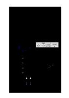
Experiment 3 : 8 Line multiplexer Procedure : 1. Ic 7415 multiplexer was installed in the logic lab breadboard. 2. 8 line multiplexer was constructed as shown in figure 3 3. Data must be set up as shown in table 3.Output LED also indications in table 3 U1
D0 D1 D2 D3 D4 D5 D6 D7 S0 S1 S2 E
4 D0 3 D1 2 D2 1 D3 15 D4 14 D5 13 D6 12 D7
LED1 ~W Y
6
LED2
5
11 A 10 B 9 C 7 ~G 74151N
INPUT E S2 S1 S0 D0 D1 D2 0 0 0 0 1 0 0 0 0 0 1 0 1 0 0 0 0 1 0 0 1 0 0 1 0 0 0 1 0 0 1 1 0 0 0 0 0 1 1 1 1 1 0 1 0 0 0 0 0 0 1 0 1 0 0 0 0 1 0 1 1 1 1 0 1 1 0 0 0 0 0 1 1 1 0 0 0
OUTPUT D3 D4 D5 D6 D70 L1 0 0 0 0 0 1 0 0 0 0 0 1 1 0 0 0 1 0 0 0 0 0 0 1 1 0 0 0 0 1 0 1 1 1 1 0 0 1 0 0 0 1 0 0 1 0 0 1 1 1 0 1 1 0 0 0 0 1 0 1 0 0 0 0 1 1 TABLE 2.
INPUTS STATEMENT D0 D1 D1 D2 D3 D3 D4 D5 D5 D6 D7
CONCLUSION: In this experiment we learn to design the function of Multiplexer and construct the internal circuitry of Multiplexer. Multiplexer is also known as the data selector. QUESTION : 1. Why is a multiplexer sometimes called a data selector Because it can control or choose inputs data to sent for control line or the input line choose to used it. 2. The circuit of a DEMUX is basically the same as for a decoder (TRUE/ FALSE)